The VLSI Lab
1. VLSI DESIGN & PROCESS SIMULATION LAB:
- Facility to design and simulate devices using 500 nm CMOS technology.
- Full-custom Application Specific Integrated Circuits (ASIC) design facility.
- Front end and Back end designing is carried out.
- Complete design flow and various types of verification are carried out like DRC, LVS and GDSII.
1.1 SOFTWARE FACILITIES:
- Cadence
- Synopsys
- Silvaco TCAD
- Mentor Graphics
- MultiSim
- Diptrace
- Tanner Tools
- UltiBoard
- PCB softwares
1.2 LAB FACILITIES:
1.2.1 ASIC FLOW
- Specification
- Architecture
- Implementation/Reuse and RTL Coding / Simulation
- Synthesis
- Timing analysis
- Floor planning, Power planning, Placement
- Design Rule Check (DRC) & Layout Vs Schematic (LVS)
- RCX and GDSII
1.2.2 PROCESS FLOW
- Mess Initialization & Wafer Identification
- Thermal Oxidation
- Threshold Voltage Adjustment
- Poly Silicon Deposition & Patterning
- Side wall Spacer Deposition & Patterning
- Source and Drain Formation
- Contact window Formation
- Metallization
2. EMBEDDED SYSTEM LABORATORY:
- Fully functional lab in terms of hardware implementation.
- Functionality is verified by implementation to FPGA / CPLD Kits
- Virtex and Spartan family kits are integral part of lab where verification is carried out.
- Lab is also equipped with DSP kits, Altium Boards, Altera boards & DACs where research on embedded application is carried out.
2.1 FACILITIES:
- Xilinx
- Chip Scope
- Altium Boards
- Model Sim
- Synplify
- Spartan kits
- Synopsys
- Active HDL
- Virtex kits
3. VLSI TECHNOLOGY LABORATORY:
- Expected to be fully functional before the start of next session.
- Laboratory consisting of the comprehensive facilities for the fabrication and testing of
silicon microcircuits of small to medium complexity. - Housed in a moderate clean room environment maintaining class 100 conditions.
- The laboratory comprises of four sections viz. Wafer Cleaning & Etching, Oxidation & Diffusion, Photolithography, Thin Film / Metal Deposition and Device Characterization.
- The main thrust is CMOS process technology.
3.1 FACILITIES
- Wafer cleaning
- Mask aligner
- Photoresist spinner
- Furnaces for thermal oxidation
- Chemical benches
- CV / IV measurements system
- Furnaces for diffusion processes
- Sputtering system for thin films deposition
- Probe station
- Hot plates / ovens for photolithography
- Microscope for visual inspection
- Device characteristics analyzer
3.2 PROCESS FLOW
- Wafer Cleaning
- Oxidation
- Photo Lithography
- Diffusion
- Photo Lithography
- Thin Film deposition
- Metallization
- Photo Lithography
- Packaging
3.3 SOME OF THE INSTRUMENTS USED FOR PROCESS FLOW IN LAB ARE SHOWN BELOW
- Wafer Cleaning
- Oxidation
- Photo Lithography
- Diffusion
- Photo Lithography
- Thin Film deposition
- Metallization
- Photo Lithography
- Packaging
| S. No. | FACILITIES | INSTRUMENTS | IMAGE |
|---|---|---|---|
| 1 | Oxidation and Diffusion | Furnaces | 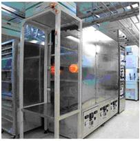 |
| 2 | Wafer Cleaning | DI Water Plant | 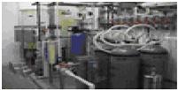 |
| 3 | Photolithography | Mask Alingner, Photoresist Spinner, Hot Plates | 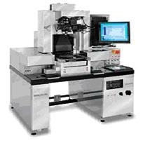 |
3.4. Oxidation and Diffusion Section
- Class 1000 room.
- Consists of three high temperature (~ 1300 C) furnaces, one is for the purpose of thermal oxidation and two others are for the purpose of the diffusion of p- and n-type dopants.
- Three clean benches facility during the loading and unloading of the wafers.
3.5. Wafer Cleaning and Etching Section
- A Class 1000 room.
- Two or three clean benches to create clean environment locally.
- Ultrasonic bath for wafer cleaning and a spinner with IR lamp for drying the wafers are part of this lab.
- Water purification RO and DI water systems for the purpose of wafer cleaning.
3.6. Photolithography
- Process includes photoresist (PR) coating, pre-baking of PR, mask-wafer aligning, PR exposing and developing.
- Requires a PR spin coater, two ovens / hot plates for pre-baking and post-baking, a UV exposure and alignment system, PR developer and rinsing solutions, and an optical microscope for inspection purpose.
3.7. Thin Film / Metal Deposition Section
- A Class 1000 room.
- Lab consists of a sputtering system for deposing the thin films of metals and insulators.
3.8. Device Characterization Section
- A Class 1000 room.
- Consist of a CV / IV measurement system, probe station, thin film thickness measurement system, wafer dicing machine and a wire bonder.
- g of the wafers.